Home / Circuits / DIY Test & measuring /
Logic probe circuit using NOR gates
This logic probe circuit using NOR gates is useful for people who need an instrument to measure the logic levels on digital circuits. This circuit is implemented with CMOS IC technology and is recommended for testing circuits using the same technology.
The voltage, required for the logic probe to work, is obtained from the circuit under test. Be careful not to reverse the voltage terminals. To avoid this problem, it is best to set the colors of each of the connecting cables. For example:
- Red for the cable that connects to the positive voltage (CN2)
- Black to the cable that goes to 0 volts. (CN3)
How does the logic probe circuit work?
The operation of this circuit is very simple. We use the CD4001 CMOS integrated circuit that has 4 two-input NOR gates, 3 LEDs, and a few passive components.
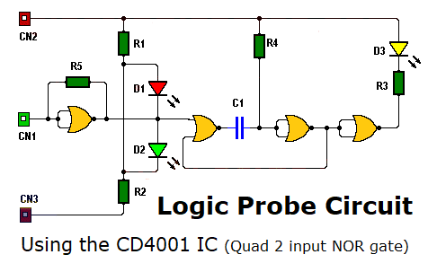
Looking at the circuit diagram. The signal we want to measure is applied to the CN1 terminal. CN1 is connected to a two-input NOR gate that behaves like a NOT or inverting gate. The inverted signal is applied to two LEDs. Which of the LEDs lights up depends on the voltage level at the output of the gate.
- When the input is high, the output of the first gate will be low, and the red LED will light up.
- When the input is low, the output of this gate will be high, and the green LED will light up.
- If there is a pulsating signal, the red and green LEDs will light slightly. When a pulsating signal is being sensed, a yellow LED will flash. This flashing is achieved using the second and third NOR gates, capacitor C1 and resistor R4. With these components, an oscillator is implemented.
The oscillator output is connected to the 4th NOR gate, wired as an inverter gate. The output of this inverter gate is connected to a yellow LED via a resistor. This oscillator is continuously triggered by the output of the first NOR gate.
The Logic probe PCB
The final use of the circuit is very important; therefore, to make its use more comfortable, an elongated printed circuit board is suggested.
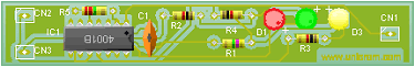

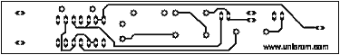
In the above picture, we see:
- The printed circuit board showing component placement.
- The printed circuit board. (copper side)
- The printed circuit board (components side)
List of circuit components for the Logic Probe
- 1 x CD4001 Integrated Circuit (4 2-input NOR gates) CMOS technology
- 3 x LEDs (1 red, 1 green, 1 yellow)
- 1 x 100 nF capacitor (C1)
- 3 x 1 K resistors (R1, R2, R3)
- 1 x 2M resistor (R5)
- 1 x 4.7 M resistor (R4)
Note: As a probe tip, you can use any sharp metal object
You may be interested in the characteristics and advantages of a logic probe.
More DIY Test & Measurement Circuits
- How do I test a Zener diode? – A simple method
- Diode tester circuit with 741
- Audible continuity tester
- Continuity tester using 741 IC
- 555 Timer tester circuit
- Op Amp Tester circuit diagram
- How to protect the 500mA fuse of a multimeter?
- How to make a current flow indicator?
- How to measure Beta of a transistor?
- Logic Probe using NOT gates
- Acoustic Logic Probe using the 555 Timer
- Logic Probe with 7 segment display
- Logic Probe circuit using CD4001 IC
- Logic Probe using two transistors
")
")

