NAND Gate
A NAND gate is also called a universal gate. This means that any other gate can be represented as a combination of these gates.
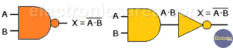
Theoretically, a two-input NAND gate can be implemented by cascading a two-input AND gate and a NOT gate (or inverter gate). See the figure below.
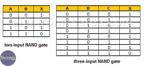
As in the case of the two-input AND gate, the same analysis can be done for the 3-input or more AND gates. As you can see, the X output is “0” only if all inputs are “1”.
NAND gate truth tables
Note: An interesting case of this type of gate. Like the NOT gate, the output X of the first and last row of the truth table has the opposite value of the inputs. In other words: A NAND logic gate can be used to obtain the behavior of a NOT gate.
Although a NAND gate appears to be the combination of two gates (an AND gate and a NOT gate), it is not. In fact, the NAND logic gate is not built by cascading an AND gate and a NOT gate, but has an independent design.
We can create a NOT gate using a NAND gate. We do this by connecting the inputs of the gate, as shown in the next figure.
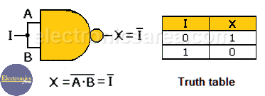
Analyzing the truth table of a two-input NAND gate, we see that there are only two cases:
- When A = B = 0, I = 1
- When A = B = 1, I = 0
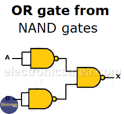
We can create a logic OR gate using NAND gates. We do this by connecting the inputs of the gate, as shown in the next figure.
In the same way, it is possible to create a NOR gate by placing a NAND gate at the output of the OR gate equivalent below.
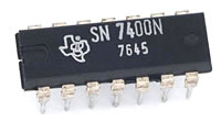
TTL SN7400N – Quad NAND Gate Integrated Circuit
You may want to know how to make NAND gate with transistors
More Digital Tutorials
- What is the difference between Analog & Digital?
- What is a logic circuit?
- Digital logic levels (high, low, 1, 0)
- The truth table
- Boolean algebra
- Karnaugh Map (K-map)
- Binary number system
- Hexadecimal numbering system
- BCD code – binary coded decimal
- Gray code – Gray code table
- Aiken code – Excess 3 code
- AND gate
- NAND gate
- OR gate
- NOR gate
- NOT gate
- XOR gate
- How to build a NAND gate with transistors & diodes?
- OR & AND logic gates made with diodes
- The combinational circuit
- The sequential circuit
- JK Flip-Flop
- What is a binary decoder?


