Home / Semiconductors /
LM117 / LM217 / LM317 variable voltage regulator characteristics
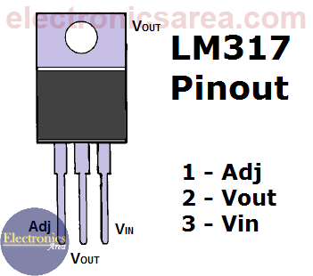
The LM317 variable voltage regulator is a 3-terminal positive voltage regulator with a 1.25 to 37-volt output voltage range. The LM317 regulator terminals are IN (input), OUT (output), and ADJ (adjust).
To achieve this voltage variation, only 2 external resistors are needed (one of them is a variable resistor). Two of the main characteristics of the LM317 voltage regulator are a current limitation and thermal protection against overloads.
How does the LM317 variable voltage regulator circuit work?
The voltage between the ADJ and OUT terminals is always 1.25 volts (voltage established internally by the regulator), and consequently, the current flowing through the resistor R1 is IR1 = V/R1 = 1.25/R1. (1)
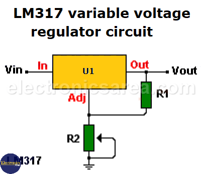
The current through resistor R1 is IR1, and it is the same current that circulates through resistor R2 (current IADJ is neglected). Then the voltage on resistor R2 is VR2 = IR1 x R2 (2)
If IR1 (1) is substituted into the formula (2), the following equation is obtained: VR2 = 1.25 x R2/R1.
Since the output voltage is Vout = VR1 + VR2, then …
Vout = 1.25 V + (1.25 x R2/R1) V… simplifying (common factor)
Vout = 1.25 V (1 + R2/R1) V.
From the last formula, it is clear that if you modify the R2 resistor value (variable resistor), the Vout voltage is modified.
- R1 = 240 ohms
- R2 = 5K or 3K (potentiometer)
The IADJ current was neglected since it has a maximum value of 100 uA and it remains constant with load and input voltage variations.
To improve the regulation, resistor R1 must be placed as close as possible to the regulator, while the R2 resistor’s ground terminal must be connected as close as possible to the ground connection of the load.
LM317 voltage regulator circuit operation improvement
In order to optimize the LM317 variable voltage regulator circuit operation, some additional elements can be incorporated into the design. See the diagram below.
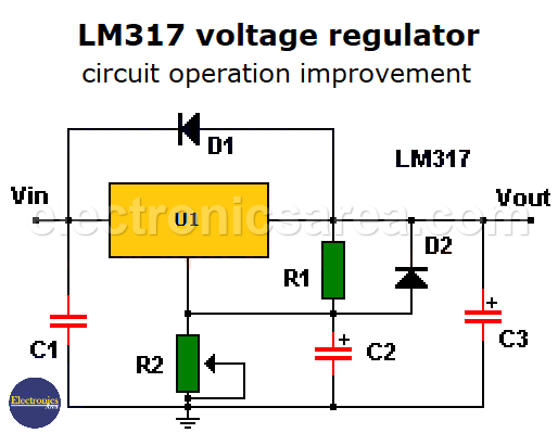
- A 0.1 μF capacitor (C1) is placed at the input terminal (IN) if the voltage regulator is away from the rectification components.
- A 1uF tantalum capacitor or a 25uF electrolytic capacitor (C3) is placed at the output terminal (OUT) to improve the transient’s response.
- A 10 uF electrolytic capacitor (C2) is placed in parallel with resistor R2 to improve rejection of the ripple voltage.
- A 1N4001 diode (D1) is placed to protect the regulator against possible short circuits at the regulator input.
- A 1N4001 diode (D2) is placed to protect the regulator against possible short circuits in its output when capacitors are discharged.
What is the difference among LM117, LM217, and LM317 voltage regulators?
- LM117 operating temperature range: -55 and 150 °C
- LM127 operating temperature range: -25 and 150 °C
- LM317 operating temperature range: 0 and 125 °C
Some regulators of this family include an additional suffix. (example: LM317K)
- Suffix K: voltage regulator with TO-3 package. Dissipates 20 W maximum with a 1.5 A current
- Suffix H: voltage regulator with TO-39 package. Dissipates 2 W maximum with a 0.5 A current
- Suffix T: voltage regulator with TO-220 package. Dissipates 20 W maximum with a 1.5 A current
- Suffix E: voltage regulator with LLC package. Dissipates 2 W maximum with a 0.5 A current
- Suffix S: voltage regulator with TO-263 package. Dissipates 4 W maximum with a 1.5 A current
You may be interested in:


