FET characteristics
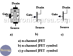
The N-channel JFET consists of a silicon bar of N-type semiconductor with two P type regions on both sides. JFET is a tri-terminal device whose terminals are called drain, source and gate.
The Outline of an n-channel JFET is described on picture (a), n-channel JFET symbol is shown on picture (b), channel JFET symbol is shown on picture (c).
JFET biasing requires that the pn junctions are reverse-biased. In order to have a current flowing through the channel, on a n-channel JFET or NJFET.
The Drain voltage must be greater than the Source voltage. In addition, to have the p-n junction reversed biased, the gate must have a more negative voltage than the source. Both cases are shown in the picture.
Main difference between JFET and BJT
Note: BJT = Bipolar Junction Transistor (NPN or PNP transistor)
The JFET electric characteristics curves are similar to the bipolar transistor curves. However, the JFET devices are controlled by a voltage, and bipolar transistors are controlled by current.
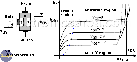
JFET has 3 main parameters:
- ID (Current flowing from drain to source),
- VGS (Gate to Source voltage) and
- VDS (Drain to Source voltage).
There are four basic operation regions: cut off, triode or Ohmic and active or saturation. We will make a brief description of each of these regions for an NJFET. (See the image above)