JFET Cutoff and Linear regions
JFET Cutoff region
In this region the current flowing from the Drain to the Source terminals of the JFET is zero (ID = 0). In this case, the voltage between the gate and the source terminals is sufficiently negative to block the flow of the current through the channel between the drain and the source terminals.
This voltage is called the pinch-off voltage and it is represented by VGS (off) or Vp.
For example, the BF245A transistor has a VGS (off) = – 2V.
JFET linear region
In this region, the JFET behaves as a nonlinear resistor. This is used in many applications where you need a voltage-controlled variable resistance.
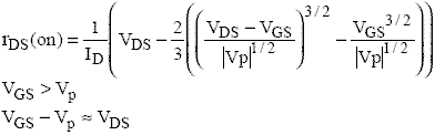
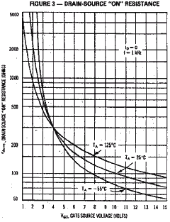
The manufacturer provides Drain-Source resistance curves (rds (on)) for different values of VGS as shown at the picture. In this region the JFET transistor has the following relationships.