What is a Schottky Diode?
The Schottky diode or Schottky Barrier Diode, unlike the semiconductor diode that has a P-N junction, has an N-Metal junction. These diodes are characterized by their switching speed and low voltage drop when they are forward biased (typically 0.25 to 0.4 volts).
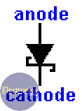
Its symbol is showed on the following diagram.
This diode works almost like the ideal diode, unlike the common semiconductor diode. However, it has some features that make it impossible to use in power applications.
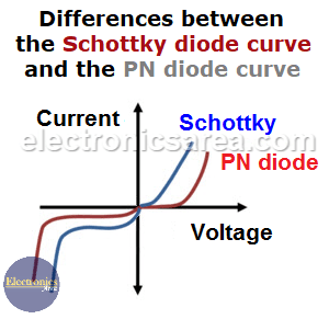
Differences between the Schottky diode curve and the PN diode curve
The common P-N diode has its curve in red and the Schottky diode has its curve in blue. It can be seen from the diagram that the Schottky diode has a lower voltage drop than that of the PN diode, when it is forward biased. It is also observed that the same happens when the diodes are reverse biased.
Schottky Barrier diode Features
- It has a small current flow capacity when it is forward biased (the current flows in the direction of the arrow of the diode). So this diode can not be used as a rectifier diode. There are rectification processes (e.g. power supplies) where the amount of current that the diode must conduct is quite large.
- It does not withstand large voltages when it is reverse biased (VCRR). However, it has numerous applications in high-speed circuits like computers circuits where high speeds are needed for switching.
Also, when it is forward biased, has a low voltage drop causing small energy consumption.
Diode Applications
- Radio frequency mixer and detector diode
- Amplitude limiting
- Power rectifier applications
- Switch
- Solar cell applications
- Used as an AND gate
- Used as an OR gate
- etc.
The Schottky diode is named after the German physicist Walter H. Schottky (23 July 1886 – 4 March 1976).


